INSPECTION METHODS
OPTICAL MICROSCOPY
Optical microscopy is a common non-destructive analysis method in electronic failure analysis. As an artificial extension to the human eye, it is possible to capture true color images of the sample at up to 1000X magnification. It can be used in conjunction with cross-sectioning in order to reveal the fine inner details of the sample. One of its main disadvantages is the narrow depth-of-field, especially at higher
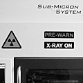
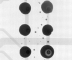
X-RAY MICROSCOPY
X-ray microscopy is a non-destructive analysis method that can reveal the inner structure of a sample, supposing the composing elements have sufficient X-ray absorption. Common applications include inspection of solder joints, wire bonds and PCB tracks. This analysis method cannot gather depth specific information from the sample. The detection of thin cracks and delaminations are only possible in special cases.
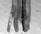
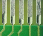
CROSS-SECTIONING
The aim of cross-sectioning is to obtain a planar section with minimal surface roughness, in order to reveal the inner structure of the sample. This allows both quantitative and qualitative investigation of dimensions and material composition with numerous microscopy techniques. One of the main disadvantages is that the method is destructive. Only one plane of the sample can be analyzed at a time.
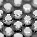
BGA DYE&PRY TEST
This is a destructive analysis method that relies on a special colorant liquid that penetrates into the existing cracks of the BGA balls. After letting the dye dry, the BGA is pried-off its PCB. Optical microscopy of the fracture surfaces can easily locate the dyed areas that are good indicators of defective solder joints. The main advantage of this technique is that it provides quick information from all of the BGA balls.
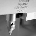
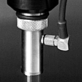
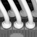
SHEAR TEST
Shear testing is a destructive analysis method for evaluating the solder joint reliability of surface mounted components. With a precision shear tool it is even possible to analyze the shear strength of individual balls on a BGA component.
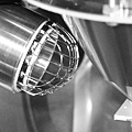
SCANNING ELECTRON MICROSCOPY
Scanning electron microscopy (SEM) allows the acquisition of high depth-of-field grayscale micrographs of the sample surface with up to 100.000X magnification. Additionally, electron probe microanalysis (EPMA, EDX) provides information about the material composition of the sample with a few µm lateral resolution. The samples need to be electrically conductive (coating is an option) before placing them into the vacuum chamber.
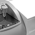
FOURIER TRANSFORM INFRARED SPECTROSCOPY
Fourier transform infrared spectroscopy (FT-IR) is an analysis method for measuring how well a sample absorbs IR light at each wavelength. The resulting spectrum represents the molecular absorption, creating a molecular ‘fingerprint’ of the sample. Like a fingerprint, no two unique samples produce the same IR spectrum. This makes FT-IR useful for the identification of unknown organic materials.
X-RAY FLUORESCENT SPECTROSCOPY
X-ray fluorescent spectroscopy (XRF) is an analysis method for determining the material composition of bulk samples. It can be used to identify elements with an atomic number greater than sodium. The lateral resolution of the analysis is worse than SEM-EDX: it is approximately 1 mm. However the samples do not have to be electrically conductive, and there is no need for them to be placed into a vacuum chamber.
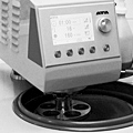
SCANNING ACOUSTIC MICROSCOPY
Scanning acoustic microscopy (SAM) is a non-destructive analysis method that can be used to image the internal structures and failures, such as delaminations, cracks, voids, of a sample. Even though this method is considered non-destructive, note that the samples have to be immersed into ionised water. One of the main advantages of this analysis method is that it can gather depth specific information from the sample.
DECAPSULATION
Acid decapsulation is an effective method to reveal the inner structures inside a plastic encapsulated component. For example dacapsulating an integrated circuit makes it possible to analyze the microwire bonds, observe defective areas on the die surface etc. It is a useful analysis method when dealing with EOS/ESD failures. There is a possibility to analyze the decapsulated samples inside a scanning electron microscope.
The most frequently used failure analysis methods are accessible in our own laboratories.
EFI-labs is part of the largest technical university in Hungary, thus we have access to more special analysis tools as well, such as:
- ion cromatography – cleanliness of PCBs
- hardness tests – material characterization
- shear and pull tests – mechanical strength of joints